July 22, 2026
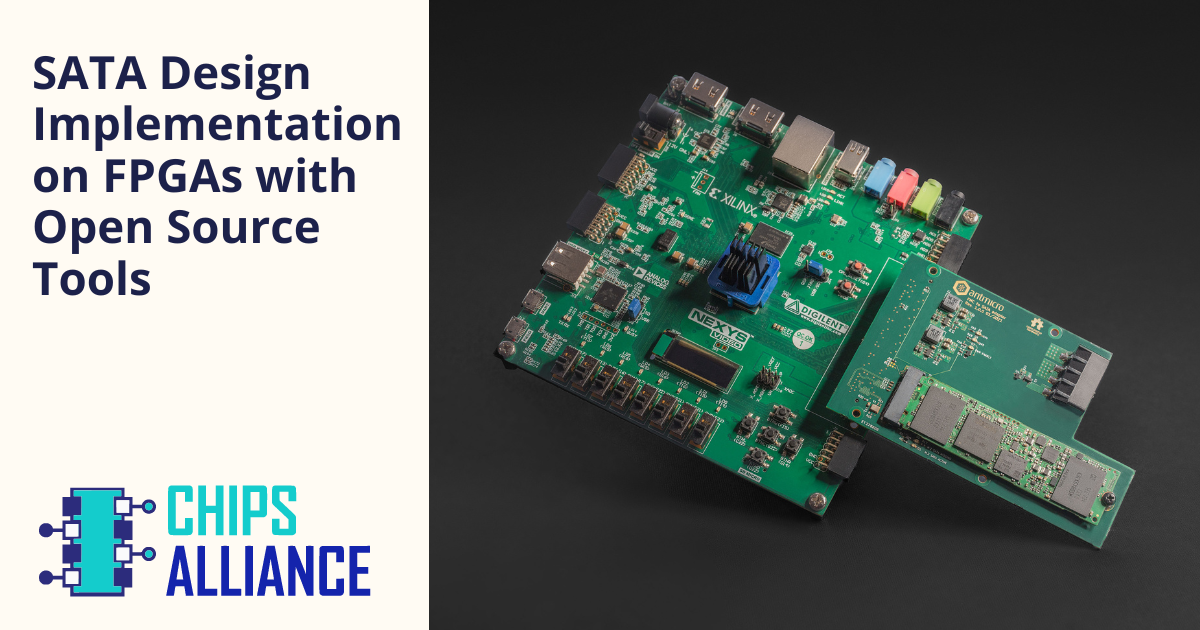
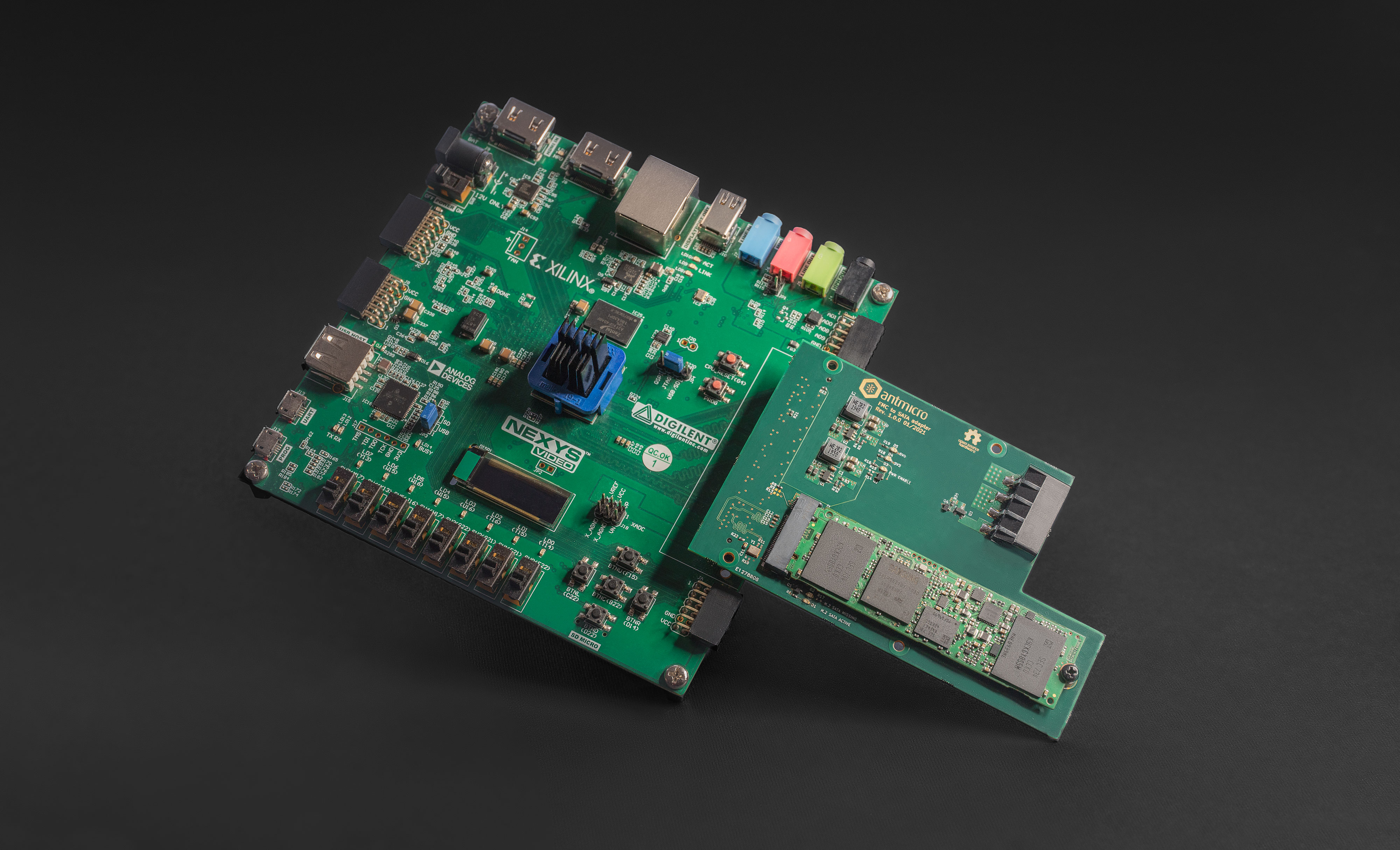
SATA Design Implementation on FPGAs with Open Source Tools
This post was originally published at Antmicro.
Real-world FPGAs designs often require high rate transmission protocols such as PCIe, USB and SATA which rely on high speed transceivers for external communication. These protocols are used to interface with various devices such as graphics cards and storage devices, and many of our clients reach out to us specifically because they need the flexibility, high-throughput and low-latency characteristics of FPGAs.
In particular, for customers that deal with high data volumes (which is very common in video applications), implementing SATA to communicate and transfer data with e.g. an SSD hard drive is a must.
Since Antmicro believes in an open source, vendor neutral approach to FPGAs, today we will describe how to build a SATA-enabled system using a completely open source flow, including the hardware platform, FPGA IP as well as, perhaps most importantly, tooling which we have been developing as part our bigger effort within CHIPS Alliance.
Origin and motivation
Antmicro is a pioneer in a software-driven approach to developing FPGAs. On top of new hardware description languages, open source IP and software that have been gaining traction in the FPGA space, one necessary missing element has been open source tooling. Open tools allow a workflow more familiar to software developers, who are used to just downloading their toolchain without having to log in anywhere or managing licenses.
Moreover, open tools provide the great advantage of easy to set up CI systems that keep track of regressions and allow more efficient and robust development.
Some of our forward-looking customers such as Google require these kinds of workflows to take full control of their development toolchain, for various reasons: security, development productivity, scale. Others, like QuickLogic, who thanks to the cooperation with us are the first ever FPGA vendor company to fully embrace open source tools, are looking to deliver a more tailored experience to their own customers, which is easier to do based on open source.
To prove the viability of open source FPGA tools, being able to implement high-speed interfaces to verify how the toolchain handles high-speed transceivers is key; thus, a fully open source SATA is a very good target, especially that an open source core, LiteSATA, was available in our favorite open source SoC generator for FPGAs, LiteX. What was missing was a hardware platform, putting it all together, and – of course – tools.
Hardware setup
The SATA design we developed is meant to run on top of a Nexys Video board from Digilent, featuring an Artix7 200T Xilinx FPGA, coupled with custom expansion board connected through the FMC connector and hosting an M.2 SSD module. Thanks to the FMC connector on the Nexys Video we achieved a relatively simple and modular hardware setup.
The FMC expansion board, developed by Antmicro, is fully open-sourced and available on GithHub.
FPGA gateware and system block diagram
The FPGA design is generated with the LiteX SoC builder and the main components that we used are:
- The VexRiscV RISC-V CPU
- The LiteDRAM controller to communicate with the DDR Memory
- The LiteSATA core to communicate with the SSD module on the custom expansion board
- a UART controller to be able to control the system from the host
Moreover, the software running in the SoC includes a simple BIOS that can perform SATA initialization and basic read and write operations of the sectors in the SSD drive.

Open source toolchain
The SATA setup proves that high speed protocols can be enabled on mainstream FPGAs such as Xilinx 7-series with an open source toolchain, with Yosys for synthesis and VPR for place and route. The LiteSATA IP core makes use of so-called GTP hard blocks, and in fact one of the main challenges we dealt with here was enabling these hard blocks in the Artix-7 architecture definition to get an end-to-end open source toolchain.
Other than enabling more coverage of popular FPGAs, much of our current FPGA toolchain effort goes into increasing the interoperability of tools like VPR and nextpnr as well as their proprietary counterparts to enable a more collaborative ecosystem which would enable the community – including universities, commercial companies, FPGA vendors and individual developers – to tackle the ambitious goal of open source FPGAs together.
For more information on the FPGA interchange and how much value it brings to the open source FPGA tooling refer to the dedicated Antmicro blog note. In the future, once that work is at a more advanced stage, LiteSATA will be one of the first example designs to be tested with the FPGA interchange-enabled tools.
Building and running the setup
The FPGA SATA design is available in the symbiflow-examples repository and can be built with the open toolchain, and run on the hardware setup described above.
After following the instructions to install the toolchain and preparing the environment, run the following to build the LiteX SATA design:
cd xc7
make TARGET=”nexys_video” -C litex_sata_demo
When the bitstream is generated, you can find it in the build directory under litex_sata_demo/build/nexys_video.
To load the bitstream on the Nexys Video board you can use the OpenFPGALoader tool, which has support for the board.
Once the bitstream is loaded on the FPGA, you can access the BIOS console through the UART connected to your host system and run the following (note that X depends on the assigned USB device):
picocom --baud 115200 /dev/ttyUSBX
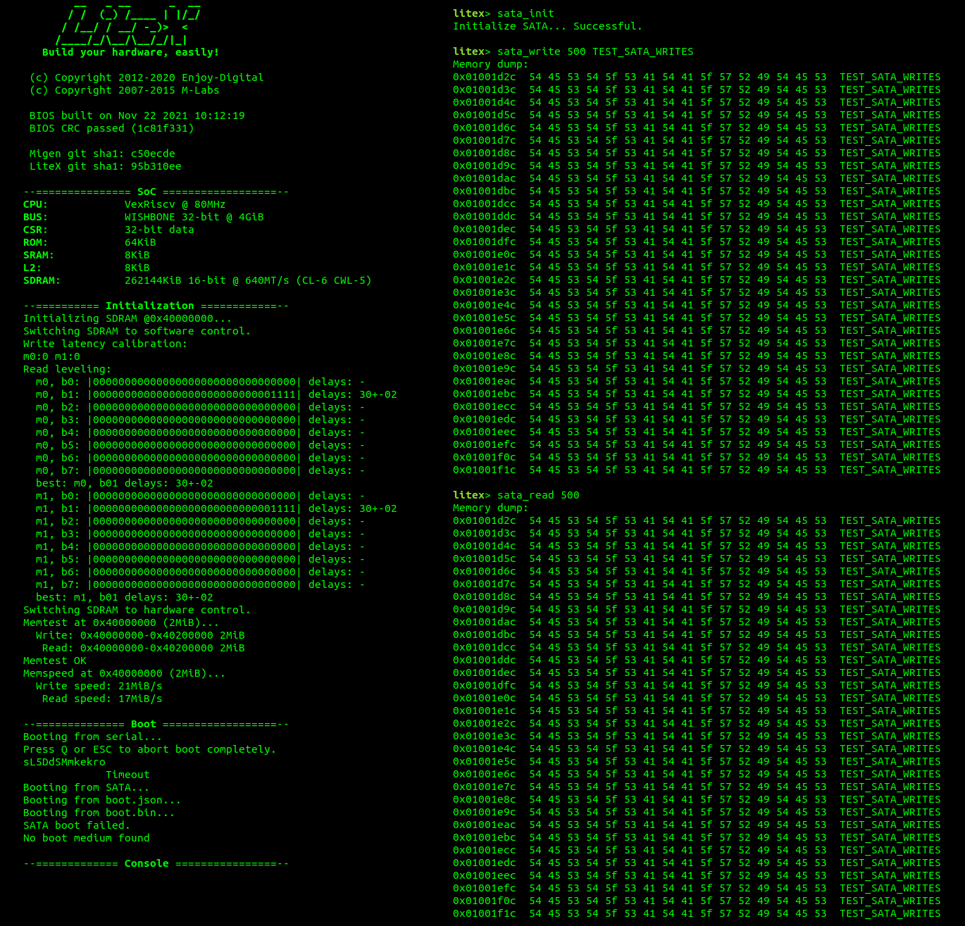
When the LiteX BIOS gives you control, you need to perform the SATA initialization before being able to read and write sectors on the drive. See the output below:
Future goals
The work on enabling the SATA protocol in a fully open source flow was one of the steps on the way towards supporting PCIe in the toolchain which will unlock even more advanced use cases. PCIe can be used for a variety of purposes, such as connecting external graphic cards or accelerators to an FPGA design, and generally enable even faster transmission rates from and to the FPGA chip.